Semiconductor wafers
A wafer is a thin slice of semiconductor material used as a substrate for electronic devices. Using deposition, doping, etching, photolithography and other techniques, devices are manufactured layer by layer. Precise measurements are made at each step as the patterned wafer moves through the fab in order to maximize yield. The wafer is ultimately diced into individual circuits which are packaged for use in electronics, solar panels, sensors and other applications.
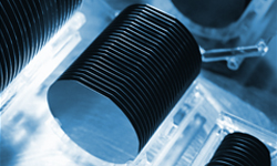
Wafers are formed of highly pure, crystalline material. A cylindrical ingot, or boule, of monocrystalline semiconductor is formed by pulling a seed crystal from a molten material. The boule is then sawn into thin slices which are polished to form individual wafers, typically ranging in size from 100-450 mm in diameter and 200–300 μm thickness.
The extremely precise manufacturing techniques required in fabricating integrated circuits place great constraints on the wafer substrates. In addition to material purity, tight tolerances are also necessary for overall flatness, site flatness (the flatness of the region where an individual device will be manufactured), and surface roughness.
4D’s AccuFiz Fizeau interferometers can measure the flatness of wafers up to 300mm in diameter, or 450mm with optional beam expanders. The unique AccuFiz D measures wafer thickness and variation at several critical wavelengths, including 1.55 microns.
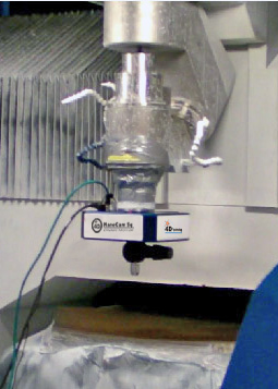
Use the NanoCam HD surface profiler to measure surface roughness on polished wafers and the manufactured features of patterned wafers.

Added Technical Resources
Measuring MEMS and other vertical roughness surfaces
A new technique provides a faster, more repeatable method for vibration-insensitive measurement in non-ideal environments.
Measuring Sub-Angstrom Roughness
How do you measure roughness with sub-angstrom precision in a noisy manufacting environment?
Read this white paper for a break-down of the options, and illustrations of the challenges presented by different solutions.
Products for Semiconductor Applications
Optical Profiling
NanoCam profilers measure surface roughness on coated and uncoated surfaces to ensure the quality of polishing processes.